Sharp 27SC26BQ Wartungshandbuch
Stöbern Sie online oder laden Sie Wartungshandbuch nach Fernseher & Monitore Sharp 27SC26BQ herunter. Sharp 27SC26BQ Service manual Benutzerhandbuch
- Seite / 42
- Inhaltsverzeichnis
- LESEZEICHEN
- SERVICE MANUAL 1
- SAFETY NOTICE 3
- (Continued) 3
- BEFORE RETURNING THE RECEIVER 3
- (Fire & Shock Hazard) 3
- CIRCUIT PROTECTION 6
- HIGH VOLTAGE CHECK 6
- 1.00 - 2 - R2 7
- A. Deflection 8
- B. Video 9
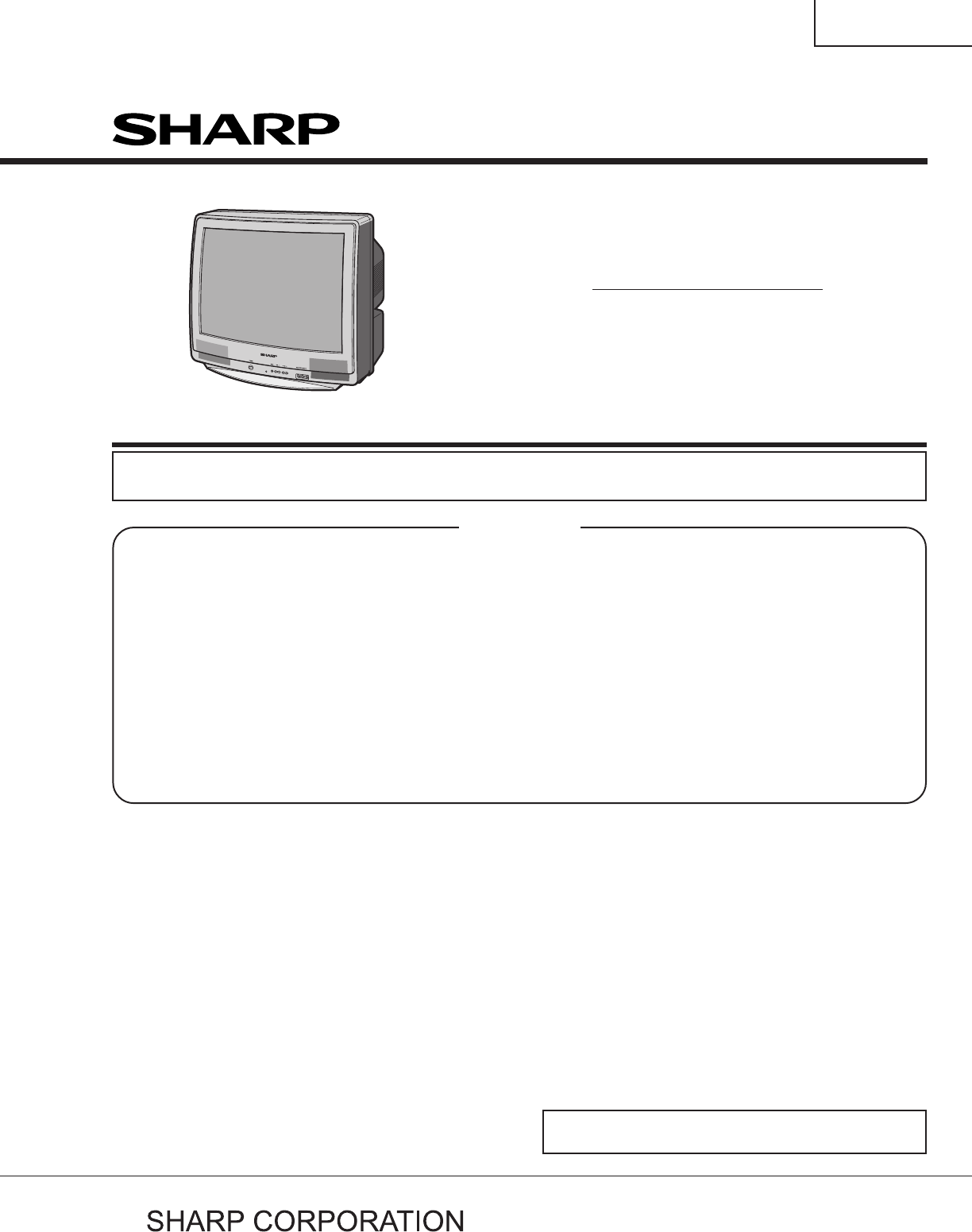
- 27SC26BQ 11
- D. Option 12
- C. Sound 12
- SERVICE ADJUSTMENT 13
- MTS ADJUSTMENT 15
- CHASSIS LAYOUT 16
- BLOCK DIAGRAM 17
- CH1 : 0.00V 18
- CH1 : 0. 0 0V 18
- SCHEMATIC DIAGRAM: CRT Unit 19
- DUNTKD872WEA1 20
- 1716 1918151413121110 21
- PWB-B: CRT Unit (Wiring Side) 30
- PARTS LIST 31
- PWB-A: DUNTKD872WEA1 32
- PWB-B: DUNTKB568WEA0 37
- PWB-D: DUNTKB572WEA1 38
- PACKING OF THE SET 40
- - M E M O 41
- ALL RIGHTS RESERVED 42
Inhaltsverzeichnis
This document has been published to be used for aftersales service only.The contents are subject to change without notice.In the interests of user-saf
10no. Item. DATA REG Range Remark Revision / ChangeV31 SHPG-YUV FIXV-TONE[02h D3]0 / 1 1V32 YDL-YUV FIXY-Delay[06h D2…D0]0 … 7 1V33 CrDL-FINE-YUV FIXC
11no. Item. DATA REG Range Remark Revision / ChangeV66 BRIGHT-OFF-AV FIXBRIGHT(OFFSET)[0Ah D7…D0]-63 … +63-5V67 CON-OFF-AV FIXCONTRAST(OFFSET)[05h D6…
12D. OptionModel27SC—O 01 SPEAKER 1O 02 FAO 1O 03 VIEW TIMER 1O 04 PON-CH 1O 05 FAV-COL 1O 06 AV3/COMPONENT 1O 07 AV 1O 08 AV2 1O 09 MTS 1O 10 TONE-CT
13SERVICE ADJUSTMENTH-VCO ADJ (I2C BUS CONTROL) (Auto &Manual Adj)• Manual Adj.1. In No Signal (RASTER) condition.2. Go to service mode, choose s
14Sub-Tint Adjustment1. Receive the half color bar signal.• RF INPUT (TU1101)2. Get into Y-Mute by R/C, or by setting the "V95" busdata to &
15Vertical-Size and Linearity Adjustments1. Receive a good local channel.(SCREEN FORMAT 4:3)2. Enter the service mode and select the serviceadjustment
16CHASSIS LAYOUT27SC26BQ
17BLOCK DIAGRAM27SC26BQ
18DESCRIPTION OF SCHEMATIC DIAGRAMSNOTES:1. The unit of resistance "ohm" is omitted.(K=kW=1000W, M=MW)2. All resistors are 1/16 watt, unl
1987109654321AB CDEFGHSCHEMATIC DIAGRAM: CRT Unit27SC26BQ
2IMPORTANT SERVICE SAFETY PRECAUTIONËService work should be performed only by qualified service technicians who arethoroughly familiar with all safety
2087109654321AB CDEFGHSCHEMATIC DIAGRAM: MAIN-1 Unit27SC26BQDUNTKD872WEA1
211716 191815141312111027SC26BQ
2287109654321AB CDEFGHSCHEMATIC DIAGRAM: MAIN-2 Unit27SC26BQ
231716 191815141312111027SC26BQ
2487109654321AB CDEFGHSCHEMATIC DIAGRAM: 2-LINE Y/C Unit27SC26BQ
251716 191815141312111027SC26BQ
2687109654321AB CDEFGHPRINTED WIRING BOARD ASSEMBLIESPWB-A: MAIN Unit (Wiring Components Side)27SC26BQ
271716 191815141312111027SC26BQ
2887109654321AB CDEFGHPWB-A: MAIN Unit (Components side)27SC26BQ
291716 191815141312111027SC26BQ
3SAFETY NOTICEMany electrical and mechanical parts in televisionreceivers have special safety-related characteristics.These characteristics are often
3087109654321AB CDEFGHPWB-D: 2-LINE Y/C Unit (Wiring Side)PWB-B: CRT Unit (Wiring Side)PWB-D: 2-LINE Y/C Unit (Chip Parts Side)27SC26BQ
PRINTED WIRING BOARD ASSEMBLIESPARTS LISTPARTS REPLACEMENTReplacement parts which have these special safety characteristicsidentified in this manual;
PWB-A: DUNTKD872WEA1MAIN UNITRef. No. Part No. Description CodeS U D653 VHDHSS4148+-1Y X Diode AAS U D654 VHDHSS4148+-1Y X Diode AAU D673 RH-DXA0
PWB-A: DUNTKD872WEA1MAIN UNITCAPACITORS [EL.··· Electrolytic, M-Poly.··· Metalized Polypro Film]Ref. No. Part No. Description CodeU C703 RC-KZ0092GE
PWB-A: DUNTKD872WEA1MAIN UNITCAPACITORS [EL.··· Electrolytic, M-Poly.··· Metalized Polypro Film]RESISTORS[M-Ox.··· Metal Oxide, M-Film ··· Metal Film]
PWB-A: DUNTKD872WEA1MAIN UNITRESISTORS[M-Ox.··· Metal Oxide, M-Film ··· Metal Film]Ref. No. Part No. Description CodeR503 VRS-CY1JF101JY X 100 1/16W
PWB-A: DUNTKD872WEA1MAIN UNITRESISTORS[M-Ox.··· Metal Oxide, M-Film ··· Metal Film]Ref. No. Part No. Description CodeR905 VRS-CY1JF104JY X 100k 1/16
PWB-A: DUNTKD872WEA1MAIN UNITRESISTORS[M-Ox.··· Metal Oxide, M-Film ··· Metal Film]Ref. No. Part No. Description CodeR3036 VRS-CY1JF102JY X 1k 1/16W
PWB-D: DUNTKB572WEA12-LINE Y/C UNITCAPACITORS [EL.··· Electrolytic, M-Poly.··· Metalized Polypro Film]PWB-B: DUNTKB568WEA0CRT UNITRESISTORS[M-Ox.··· M
MISCELLANEOUS PARTSCABINET PARTS1-31-41-51-1 11-22Ref. No. Part No. Description CodeVSP9050PB35WA X Speaker (L) AHVSP9050PB35WA X Speaker (R) AHQCNW
4Precautions for using lead-free solder1 Employing lead-free solder"PWBs" of this model employs lead-free solder. The LF symbol indicates le
40PACKING OF THE SETFRONTREARUse tape tofix the top side ofpacking case.Use 12 staples tofix the bottom sideof packing case.27SC26BQ
41- M E M O -27SC26BQ
COPYRIGHT © 2007 BY SHARP CORPORATIONNo part of this publication may be reproduced,stored in a retrieval system, or transmitted inany form or by any m
5LOCATION OF USER'S CONTROLFront PanelVOLUME UP/DOWN (k) Increases sound.(l) Decreases sound.CHANNEL UP/DOWN(a) Selects next higher channel.(s)
6CIRCUIT PROTECTIONThe receiver is protected by a 4.0A fuse (F701),mounted on PWB-A, wired into one side of the ACline input.X-RADIATION PROTECTOR CIR
7For adjustments of this model, the bus data is converted to various analog signals by the D/A convertercircuit.Note: There are still a few analog adj
8A. Deflectionno. Item. DATA REG Range Remark Revision / ChangeD01 V-SHIFT FIXV-SHIFT[13h D2…D0]0 … 7 0D02 H-SHIFT ADJH-PHASE[16h D4…D0]0 … 31 H-PHASE
9B. VideoTV-Picture-AdjDTV-Picture-Adjno. Item. DATA REG Range Remark Revision / ChangeV01 SUB-CON ADJCONTRAST[05h D6…D0]0 … 127PIC.DTVV02 SUB-TINT AD
Verwandte Produkte und Handbücher für Fernseher & Monitore Sharp 27SC26BQ

 (76 Seiten)
© 2020, manymanuals.de. Alle Rechte vorbehalten. | 0.044 s |
 Manymanuals.com
 Manymanuals.de
 Manymanuals.fr
 Manymanuals.it
 Manymanuals.pl
 Manymanuals.cz
 Manymanuals.es
 Manymanuals-pt.com
Kommentare zu diesen Handbüchern